Board Overview
The ESP32-S3-Touch-LCD-4.3 (Type B) packs a remarkable density of functionality onto a 112.4 x 75.1 mm PCB. Understanding where each component sits and how the subsystems interconnect is the first step toward making effective use of the board — whether you are building a CAN-connected HMI panel, an RS-485 data logger, or a battery-powered touch interface for field deployment.
Board Components
Section titled “Board Components”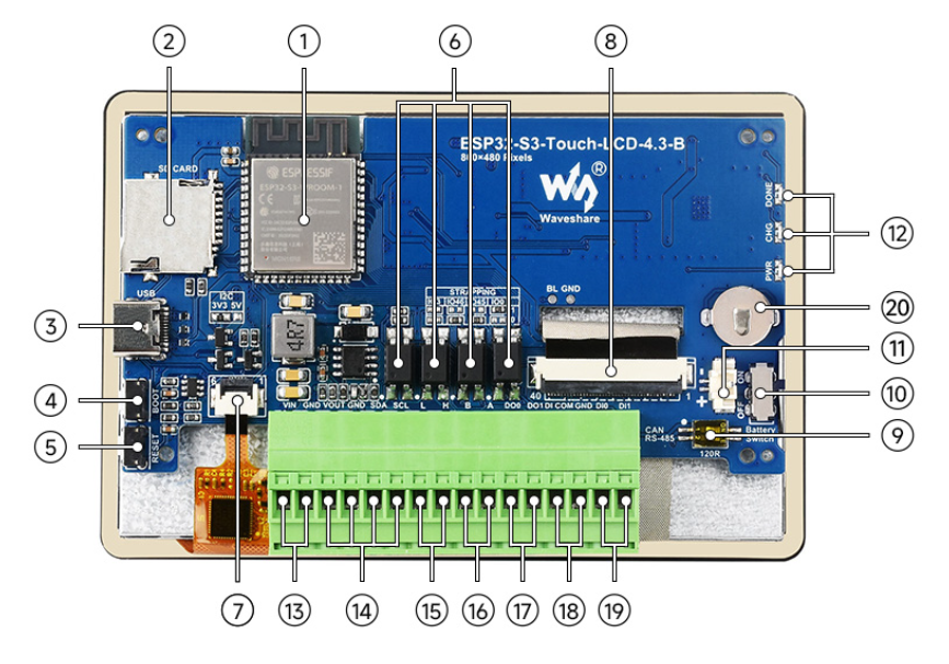
Image credit: Waveshare
The following list identifies every major IC, connector, and control element on the PCB. The numbering corresponds to the silkscreen reference designators visible on the board itself.
- ESP32-S3-WROOM-1-N16R8 — The main system-on-chip module from Espressif, housing dual Xtensa LX7 cores at 240 MHz, 2.4 GHz WiFi 802.11 b/g/n, Bluetooth 5.0 LE, 16 MB of quad SPI flash, and 8 MB of octal PSRAM. The module’s PCB antenna occupies one corner of the board.
- SGM2212-3.3 — An 800 mA low-noise low-dropout linear regulator that steps the 5V power bus down to the 3.3V rail supplying the ESP32-S3 module and all digital logic ICs.
- FSUSB42UMX — A USB 2.0 high-speed analog multiplexer that switches the ESP32-S3’s USB data lines between the UART programming port (via CH343P) and the native USB Host/OTG port. The CH422G IO expander controls which path is active.
- Touch panel connector — A 40-pin FPC connector carrying the GT911 capacitive touch digitizer signals from the display assembly.
- USB-to-UART Type-C port (Type-C2, top edge) — The primary programming interface. Connected through the CH343P USB-to-UART bridge, this port handles firmware flashing and serial debug output.
- USB Type-C port (Type-C1, side edge) — Native USB Host/OTG port routed through the FSUSB42 multiplexer to GPIO19 (D-) and GPIO20 (D+). Suitable for USB peripherals, CDC serial, or MSC device modes.
- TJA1051T/3/1J — A 3.3V CAN bus transceiver conforming to ISO 11898-2. It translates the ESP32-S3’s TWAI peripheral signals into differential CAN bus levels, with the physical interface exposed on a 3-pin screw terminal.
- CH422G — An I2C IO expander that serves as the board’s central control hub. It manages LCD backlight enable, touch controller reset, SD card chip select, USB multiplexer selection, and the optocoupler-isolated digital I/O channels — all from a pair of I2C lines shared with the touch controller and RTC.
- BOOT button — Hold this button while pressing RESET (or during power-on) to force the ESP32-S3 into UART download mode for firmware flashing.
- RESET button — Pulls the EN pin low to perform a hard reset of the ESP32-S3 module.
- MP3302DJ-LF-Z — A boost-topology LED driver that converts the 5V rail to the voltage required by the display backlight LEDs. Output current is set by resistor R8, with a factory default of 580 mA at 1.2 K ohms.
- 4.3” display panel connector (PORT1) — A 40-pin FPC connector carrying the 16-bit RGB565 parallel data bus, sync signals, and backlight power to the ST7262-controlled IPS panel.
- TF card slot — A push-push microSD card socket operating in SPI mode. The chip select line routes through the CH422G expander (EXIO4) rather than a dedicated GPIO.
- Sensor header — A pin header exposing an ADC-capable GPIO for connecting analog sensors such as thermistors, potentiometers, or 4-20 mA loop receivers (with appropriate signal conditioning).
- CAN header (J7) — A 3-pin screw terminal block carrying CANH, CANL, and GND. Accepts 20-16 AWG wire for direct field connection to a CAN bus segment.
- I2C header — An expansion header breaking out SDA, SCL, and I2C_VCC for connecting external I2C peripherals such as environmental sensors, EEPROMs, or additional IO expanders.
- RS-485 header (J1) — A 3-pin screw terminal block carrying A, B, and GND for half-duplex RS-485 communication. Accepts standard twisted-pair field wiring.
- 3.7V Li-Po battery connector — An MX1.25 2-pin connector (PH2.0 on some production variants) for a single-cell 3.7V lithium polymer battery. The CS8501 manages charging and boost conversion.
- CAN terminal resistor selection jumper — A solder jumper that connects a 120 ohm termination resistor across CANH and CANL. Default position is OFF (open). Close this jumper only when the board sits at a physical end of the CAN bus.
- RS-485 terminal resistor selection jumper — A solder jumper enabling a 120 ohm termination resistor between the A and B lines. Default position is OFF. Enable only at bus endpoints.
- CH343P — A USB-to-UART bridge IC from WCH that provides reliable serial communication between the Type-C2 programming port and the ESP32-S3’s UART0 (IO43 TX, IO44 RX).
- SP3485 — A 3.3V RS-485 transceiver supporting half-duplex communication at up to 10 Mbps. The board’s hardware-controlled TX/RX direction switching means no additional GPIO is needed for bus direction control.
- CS8501 — A Li-Po battery charge and discharge management IC. It handles constant-current/constant-voltage charging from the 5V bus and provides boost conversion from battery voltage back to 5V when external power is removed, enabling seamless power transitions.
- PCF85063A — A real-time clock IC with a CR927 coin cell backup battery holder (Type B variant only). Connected to the shared I2C bus at address 0x51, it maintains date and time across power cycles and deep sleep states.
- Status LEDs — Three indicator LEDs visible along the board edge: PWR (power present on the 5V rail), CHG (Li-Po charging in progress), and DONE (charge cycle complete).
Subsystems Overview
Section titled “Subsystems Overview”The board’s functionality divides into five interconnected subsystems, each built from the components listed above. Understanding these groupings clarifies which resources are shared and where contention can arise.
Display Subsystem
Section titled “Display Subsystem”The visual output chain begins at the ESP32-S3’s RGB LCD peripheral, which drives a 16-bit parallel interface (RGB565) to the ST7262 controller embedded in the 4.3” IPS panel. Nineteen GPIO pins carry the pixel data, sync signals (HSYNC, VSYNC), data enable (DE), and pixel clock (PCLK) — making the display the single largest consumer of GPIO resources on the board. The frame buffer lives in PSRAM, and the ST7262 handles the conversion from parallel data stream to active-matrix panel drive signals.
Touch input flows through the GT911 capacitive controller, which sits on the shared I2C bus at address 0x5D. The GT911 generates an interrupt on IO4 when a touch event occurs, and its hardware reset line routes through the CH422G expander (EXIO1) rather than consuming an additional ESP32-S3 GPIO.
The backlight uses a separate power path entirely. The MP3302DJ boost converter steps the 5V rail up to the voltage demanded by the LED string, with output current governed by resistor R8. The CH422G controls backlight enable via EXIO2, providing software-driven on/off switching without PWM dimming (though the MP3302DJ’s shutdown pin could be driven with a PWM signal for brightness control in custom modifications).
Communication Interfaces
Section titled “Communication Interfaces”Two industrial serial buses share the board’s edge connectors. The CAN interface routes through the TJA1051T transceiver, translating the ESP32-S3’s native TWAI peripheral (IO15 TX, IO16 RX) into ISO 11898-2 differential signaling on the J7 screw terminal. The RS-485 interface uses the SP3485 transceiver on UART0 (IO43 TX, IO44 RX), with automatic direction control eliminating the need for a dedicated DE/RE GPIO. Both interfaces expose solder jumpers for optional 120 ohm termination resistors — these should be enabled only at the two physical endpoints of each bus segment.
IO Expansion
Section titled “IO Expansion”The CH422G I2C IO expander is arguably the most architecturally significant component on the board after the ESP32-S3 itself. It occupies I2C addresses 0x20 through 0x27 and provides the control signals that would otherwise require eight additional GPIOs: touch controller reset (EXIO1), LCD backlight enable (EXIO2), LCD reset (EXIO3), SD card chip select (EXIO4), and USB multiplexer selection (EXIO5). On the Type B variant, remaining pins serve as the interface to optocoupler-isolated digital inputs and outputs, enabling direct connection to industrial-voltage signals without risking the ESP32-S3.
Power Distribution
Section titled “Power Distribution”The board accepts power from three possible sources: USB 5V from either Type-C port, a 7-36V wide-range DC input (Type B only), or a 3.7V Li-Po battery through the MX1.25 connector. The CS8501 manages the interplay between external power and battery, providing seamless switchover and charge management. The SGM2212 LDO produces the 3.3V rail from the 5V bus, while the MP3302DJ generates the backlight drive voltage from that same 5V source. A separate I2C_VCC rail powers the I2C bus pullups and certain peripherals independently.
USB Topology
Section titled “USB Topology”Dual USB Type-C ports serve distinct roles. The top-edge Type-C2 port connects through the CH343P UART bridge for firmware flashing and serial debug — this is the port you will use most during development. The side-edge Type-C1 port provides native USB access to GPIO19/GPIO20 for Host or OTG operation. The FSUSB42 analog multiplexer sits between the ESP32-S3’s USB data pins and these two ports, with the CH422G controlling which path is active via EXIO5. Only one USB mode can be active at a time.
Board Dimensions
Section titled “Board Dimensions”The bare PCB measures 112.4 x 75.1 mm, with four M3 mounting holes positioned for secure enclosure mounting. When fitted inside the optional acrylic or aluminum casing, the overall footprint grows to 116.3 x 79 mm. The display active area occupies 95.54 x 54.36 mm of the front surface, with a total viewable area slightly larger due to the IPS panel’s border region.
| Dimension | Measurement |
|---|---|
| PCB width | 112.4 mm |
| PCB height | 75.1 mm |
| Cased width | 116.3 mm |
| Cased height | 79.0 mm |
| Display active area | 95.54 x 54.36 mm |
| Mounting holes | M3.0, four corners |
| PCB thickness | 1.6 mm |